![<?echo $_SERVER['SERVER_NAME'];?>](/template/twentyseventeen/skin/images/header.jpg)
In the era of continuous development of science and technology, the micro-nano-functionalization of the functional structure can not only bring energy and raw material savings, but also achieve high integration of multi-function and greatly reduce production costs. Micro-nano processing technology is mainly divided into direct processing technology and graphics transfer technology. Direct processing techniques include laser processing, focused ion beam (FIB) etching, Local Anodic Oxidation local anodizing (AFM based), Dip Pen NanoLithography dip pen nanomachining etching, etc.; graphics transfer technology is mainly divided into three parts: film Deposition, graphic imaging (essential), graphics transfer. As the core of the micro-nano processing technology, the graphics generation process can be divided into three types: (1) planar graphics process, probe patterning process, and model graphic process. The core of the planar patterning process is parallel imaging characteristics, including lithography (mask, direct write), electron beam exposure (EBL); (2) probe patterning process using high-precision probes for samples or coatings Perform point-by-point scanning imaging technology with high precision, partial direct writing, 3D processing, etc. Representative technologies include: Thermal Scanning Probe Technology (NanoFrazor); (3) Model Graphical Process is reproduced using micro-nano-sized molds The corresponding micro-nanostructure, the typical process is nanoimprint technology (NIL), and also includes molding and molding techniques.
Although there are many micro-nano processing technologies, the only structural processing that can achieve nano-scale (less than 100 nm) resolution is: focused ion beam etching (FIB), nanoimprint technology (NIL) and electron beam exposure (EBL). Focused ion beam etching (FIB) uses the focused ion beam to strike the surface of the material and achieve the purpose of removing the matrix material. It can realize 3D nanostructure direct writing, and the applicable materials are wide, but the processing precision is not high. The nanoimprint NIL adopts nanometer. The microstructured template transfers the graphics on it to other materials, which is highly efficient, but the template itself needs other process preparation. EBL is generally used. The template is expensive and cannot be modified. It is suitable for mass production; electron beam exposure uses focused electrons. The bundle is modified by colloid and can be processed up to 10 nm with high precision. It is a model of traditional high-precision machining, but it is expensive and complicated to operate. The proximity effect makes the two structures inaccessible.
Swiss-based Swisslitho's 3D nanostructured high-speed direct-write machine NanoFrazor uses the thermal probe scanning and writing technology developed by IBM Zurich Research Center and the new direct-write glue technology to innovate the thermal probe-based nanostructure writing and cold probe based. The combination of topography and readout enables high-precision 3D nanostructure direct write and real-time topography detection. This technological innovation won the 2015 R&D top 100 award from R&D Magazine. NanoFrazor is the latest technology in nanofabrication with its 10 nm machining accuracy and 0.1 nm accuracy profile detection capability.
NanoFrazor technical features:
Back thermal scanning probe:
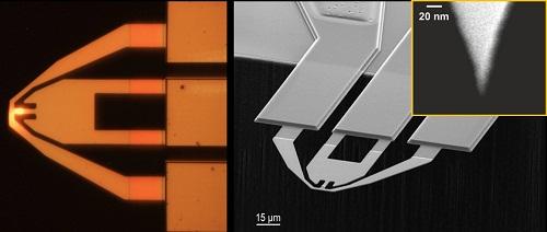
Swisslitho uses a special cutting-edge process to prepare a back-heated direct write probe from Si material with a probe tip tip diameter of less than 5 nm (Figure 1). Localized heating under voltage control is achieved by changing the doping amount in the back region of the tip, while the other positions of the probe are unaffected. The temperature in the heating zone is up to 1000 ° C and the tip temperature can be 300-600 ° C. The probe side arm is designed with a thermal sensor for topography detection with a topographical detection accuracy of up to 0.1 nm.
Excellent performance of direct writing adhesive PPA:
The PPA direct-resistance (resist) developed by IBM Zurich Laboratory for nanofabrication is characterized in that when the temperature is higher than 150 °C, PPA will be decomposed into organic molecular monomers by heat and discharged with the protective gas. When the heated probe is close to the PPA to a certain range, the PPA near the tip of the needle will be instantaneously decomposed into gas molecules, leaving a hole in the shape of a needle tip, and the portion around the hole is not affected by the low thermal conductivity of the PPA. Effectively avoiding the melting accumulation effect of common polymer materials affecting resolution and tip life. The combination of holes of a plurality of probes forms a high-precision pattern, and the processing of the 3D nanostructure can be realized by controlling the depth of the lower needle.
NanoFrazor written nanostructure appreciation:
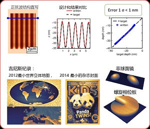
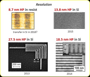
3D high speed direct writing structure and world Guinness record
Preparation of periodic structures on PPA paste and Si substrates
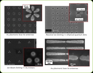
NanoFrazor has no proximity effect, making it easy to prepare adjacent nanostructures such as bow antennas and periodic structures
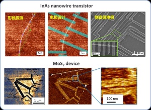
NanoFrazor can realize the positioning and morphology observation of nano-wires, two-dimensional materials after coating, and implement specific direction design.
The realization of the functional structure micro-nano-based is based on advanced micro-nano processing technology. The improvement and optimization of more technical details in micro-nano processing is the technical direction that research and field equipment manufacturers are constantly pursuing. NanoFrazor is also constantly trying to be more precise. More convenient, become a more cost-effective, more powerful 3D direct writing device.
About Quantum Design
Quantum Design is the world's leading manufacturer and distributor of scientific equipment and was founded in 1982 in San Diego, California. The company's SQUID Magnetic Measurement System (MPMS) and Material Integrated Physical Property Measurement System (PPMS) have become the world's recognized top-level measurement platform, widely distributed in the world's most research-oriented fields of materials, physics, chemistry, nanotechnology, etc. laboratory. In 2007, Quantum Design acquired LOT, the largest instrument distributor in Europe, and has become a world-renowned multinational company in the field of scientific instruments. At present, the company has dozens of branches and offices in the United Kingdom, the United States, France, Germany, Brazil, India, Japan and China, and operates in more than 100 countries and regions around the world. China is the most active market for Quantum Design, with offices or offices in Beijing, Shanghai and Guangzhou. Over the past decades, the company has achieved fruitful cooperation with China's research and education fields, providing advanced equipment and high-quality services for the advancement of Chinese scientific research.
It's a TV cabinet of home office storage, made of cold-rolled steel, tall legs with locking doors. You can put it in the living room, bedroom, kitchen, or bathroom to keep sundries, or as a display areal for photo frames, vases and green plants.
With an adjustable shelf, you can adjust the height as you need.
Completely coated surface, rust-free and anti-corrosion, it's easy to clean.
Some types with locks can protect your privacy.
You can assemble the TV metal locker cabinet easily with a detailed manual and complete screws.
If you are looking for a metal locker TV stand for sale, it is your choice!
Metal Cabinet Tv Stand,Metal Tv Cabinet,Black Metal Tv Cabinet
LUOYANG SHIDIU IMPORT AND EXPORT CO., LTD , https://www.shidiucabinets.com